|
Vaughan Family Timestream® Maps |
| Home Biography People Places Multimedia: Making It Work On the Water Writings/Presentations |
Birthing Microchips
by Tay Vaughan
From Digital Deli
The Comprehensive, User-Lovable Menu of Computer Lore, Culture, Lifestyles and Fancy
by The Lunch Group & Guests
Edited by Steve Ditlea
Published 1984
Note: Digital Deli is copyright ©1984. It is posted on www.atariarchives.org with the approval of Steve Ditlea, editor of the book, for archival purposes only. Commercial reproduction or use of any of this material without the permission of the individual author and/or photographer is prohibited.
Tay Vaughan is a senior scientist at ACI Engineering Consultants. He has a Coast Guard captain's license, flies airplanes and plays the cello when he is not busy making clean rooms even cleaner.
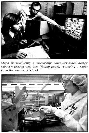
testing new dies
E-beams, plasma etchers, gold evaporators, scanning electron microscopes, four-stack furnaces, spintrack developers and ion implanters: these are just some of the highly specialized tools that fill the "clean rooms" where microprocessors and other integrated computer circuits are made. This equipment allows computer scientists to work within the scale of microns (one micron equals one millionth of a meter) and perform the optical procedures and chemistries required of the fabrication process.
Integrated circuits consist of layers that manifest specific electrical properties, each layer etched with a carefully designed microscopic pattern of lines and junctions to carry or manipulate electrical voltages. The smaller the width of the etched lines, the more lines can be squeezed onto a chip. The shorter the distance between connections, the faster things can happen. Computer operating speeds are measured in nanoseconds, or billionths of a second.
Microchips begin as thin, round wafers of pure silicon, a half-millimeter thick, cut from carefully grown crystal columns up to six inches in diameter. The wafers are polished to a flat surface, and interferometers check for planar evenness using parallel surfacing techniques that measure tolerances in terms of angstroms. (There are ten thousand angstroms in a micron.)
Highly paid designers initiate the manufacturing process, playing color-coded computer-assisted design (CAD) machines like three-dimensional chess masters at a tournament. A common chip may have from eight to twelve layers of interlocked tracery of conductive, semiconductive or nonconductive material. The patterns of lines and junctions for each layer (as well as the materials themselves) are determined by the requirements and function of the specific microdevice as well by the limits of planar geometry. Most layers must interconnect with the layer above and/or the layer below. While children may learn to draw the outline of a house without lifting pencil from paper or crossing an existing line, microchip designers draw entire cities replete with roadways and subways following the same strict rules.
The CAD system prints out large-scale drawings of a microchip's tracery, layer by layer. After each layer's drawing has been carefully checked manually, often on a large floor where scientists crawl about on hands and knees searching for errors, photo masks are made.
Microchip manufacture is a photoetching process with roots in both transistor and printed circuit technologies. But no longer must photographs of each layer of circuitry be painstakingly reduced from full-size drawings to microscopic dimensions. Just as most newspapers use word-processed data for typesetting, refined computer data from the CAD system can directly guide a powerful beam of electrons to etch the required pattern of lines needed for each layer.
Photoetching remains, however, at the heart of microchip manufacture, and it is a "wet process" fabrication system. To etch various layers of a chip, these are covered with a layer of photoresist, a liquid coating that, when dry, reacts to certain colors of light or to a beam of electrons. Exposed photoresist can then be washed away with developers (or will remain, depending on whether a positive or negative solution is specified and depending on the "recipe" used).
Particularly in prototype laboratories, there is a great deal of hand developing. Many process engineers are therefore quite finicky, like testy French chefs at a five-star restaurant. Using vacuum wands, our chefs carry wafers back and forth between spinners, coaters and special drying ovens. Some have an intuitive sense about the sheen being just right or the oven a little too hot, and they will hover over their work, tweaking dials, adjusting and perfecting. Wet-process chemistry is an art.
Electron-beam (E-beam) equipment occupies a singularly important position in the panoply of instruments and apparata seen on the wafer fabrication floor. This equipment, the chefs finest carving knife, draws the patterns upon which all else in the production process is dependent. Costing over a million dollars, E-beam machinery is supplied with its own dedicated environmental chamber even within the clean room.
Steps in production
Where photoresist does not cover the substrate, acids etch the material, carving channels and lagoons which, in the subsequent layering step of fabrication, can be filled with conductive metals or other esoteric materials called for by the recipe.
Ion implanters are used to "dope" layers with impurities by shooting molecules at the surface under high vacuum conditions. Diffusion furnaces coat molecules onto the surface of the wafer using violent chemicals and natural molecular affinities at temperatures exceeding 1,500 degrees Fahrenheit. Furnaces can also remove selected molecules in a bath of hot oxygen. Silicon itself is layered by epitaxy. Pure silicon is an insulator, doped silicon is semiconductive, and aluminum oxide (among other metals used in microchips) is conductive.
Carefully following the recipe, process chefs expose the photoresist-covered substrate. They develop it. They etch away unwanted portions. They build up a layer of silicon. They dope it. They cover this with more photoresist, then expose, develop, etch, coat, bake, expose, develop and bake some more. The combinations and protocols are myriad in this painstaking layer-by-layer fabrication process. It can take as many as six weeks to fabricate a microchip. Each step of the recipe requires handling, and some steps-particularly in the diffusion furnaces-require many hours while molecules attach to molecules according to nature's inexorable laws.
|
CLEAN ROOMS - A sidebar
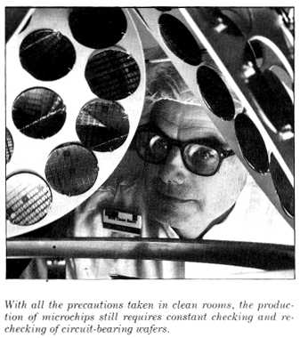
The Class 10 clean rooms are on the order of eight hundred to a thousand times freer of particulate matter than a hospital operating room. Here there are fewer than ten motes of anything larger than a half-micron in diameter per each cubic foot of air. A hundred thousand cubic feet of filtered, humidified and temperature-controlled air pushed into the room each minute is enough to quickly remove the odors and dust of everyday life. An entire ceiling of high-efficiency particulate air (HEPA) filters traps all but the minutest contaminants. Air drains out through grates in the floor or along the lower walls, carrying with it such detritus as the 15-micron epithelial cells and other particles naturally sloughed from the skin of workers. Pencils are prohibited here because invisible airborne graphite particles not only are "large," but are also efficient electrical conductors and can therefore short-circuit the fine lines of a microchip template in production. Computer-controlled cooling coils, humidifiers and automatic dampers regulate this environment. Variation by a single degree of temperature can destroy a week's work. And the 120 decibels of sound energy at the fan motor itself is reduced from loudness at the threshold of pain to the quiet of a concert hall after flowing with the air through specially manufacturered anechoic and attenuating chambers and through insulated ducts large enough to walk in. Lowfrequency airborne noise can rumble the fine optical equipment and frustrate alignment. People speak softly in the clean room. T.V. |
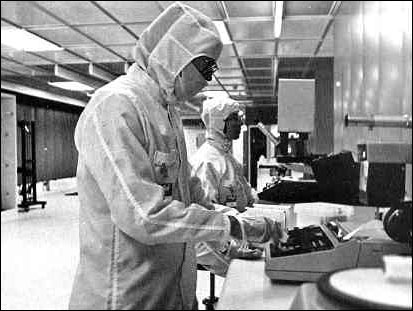
 Looking through plate-glass partitions into Class 10 clean rooms where microchips are made is an awesome first-time experience. Gowned, goggled, hooded and masked workers hunch over strange, sleek machines or stand about in small groups before complex computer keyboards and dedicated monitors.
A back-lapper removes much of the finished wafer's thickness and reduces its weight. A diamond cutter is then used to carve out each individual die, a diebonder fastens the chip to a pattern of interconnects, and the chips are encased in plastic. Leads are attached, using special soldering techniques, and the finished microchip is packaged for shipment. This finishing process requires a great deal of handwork, and for this reason much assembly is performed in areas of the world where labor rates are cheap. A single container of microchips air-freighted abroad has perhaps the highest value-to-weight ratio of any commodity in present-day world commerce.
Under the most trying conditions and with demanding high-resolution requirements, some chefs in the prototype lab might be pleased with a yield of a single working microchip per hundred dies on a wafer. So many things can go wrong. But yields are an important consideration to a company's profit margin. Normally, if 30 to 40 percent of the chips on a wafer perform as desired, the yield is considered good. If 80 percent work, yield is considered excellent. (Bad chips go into a trash bin and are eventually buried at the city refuse dump for anthropologists a millennium hence to unearth and reverse-engineer in order to make pronouncements upon today's state of the art.)
Throughout the fabrication process, the wafer and dies are tested. This quality control is critical for efficient, economic production because contaminants are everywhere in the process (though in most cases are controllable). Vibration is reduced by separating and isolating the specially engineered wafer fabrication areas from the rest of the facility and by carefully balancing air supply and mechanical systems. Equipment floats on air bags and springs. Ductwork and piping inside the building is specially designed. There is no clanging of hot-water pipes in a wafer fabrication facility.
Microchip manufacturing technology faces a limit of scale. To further reduce line width to submicron dimensions in order to produce very large-scale integrated circuits (VLSI) and to stack many more layers of very compact lines in the vertical architecture required by very high-speed integrated circuits (VHSIC), breakthroughs are required. Wet processing must be done away with. At widths of a micron, photoengraving can cause lines that are too narrow or too wide or troughs too deep or dangerously undercut by etching "in all directions."
To avoid the wet process entirely, the E-beam is being used for "direct-write" etching because it can deliver very fine line resolution. It is difficult, however, to control its energy level and the depth of its cut. Impetuously, it hacks and hews into substrate layers and can destroy many days of cumulative effort by cutting into layers below.
Laser writing techniques are being developed that provide not only highly accurate direct-write resolution but also some control of depth. Not available yet are molecular beam systems that allow great control of impact velocity. With heavy molecules bombarding a substrate, velocity can be altered the way a sand-blaster alters air pressure to do fine detailed work, thus achieving high resolution.
The manufacture of microchips is indeed a study of scale. As the scale becomes smaller and smaller, the very molecular fabric of the device itself and its electrical properties change, imposing finite design limits. The engineers without blinders who are working at the technological threshold claim "You can't say can't" about anything, and they constantly scan the edges of their peripheral vision for solutions of scale. Ultimately, it may be that microchips as they are known today will be outmoded by other techniques of voltage amplication and information management that are more appropriate to submicron or angstrom scales.
|
ON SILICON - A sidebar Though silicon is the second most common element on the earth's surface, constituting close to one-quarter of its rocky crust, few people outside the microchip industry have ever seen it in its pure, dark gray crystalline form. In nature, silicon is found only in combination with other elements, forming common minerals like quartz and flint (in fact, its name derives from silex, Latin for "flint"). In industry, compounds of silicon (rhymes with "silly Khan") are used to make glass, ceramics, enamels and dyes. Synthetic silicon oxides known as silicones (pronounced like "silly Cones") are employed as lubricants and waterproofing compounds and to make rubber that is chemically inert-hence the use of these oxides in prosthesis and plastic surgery. To produce pure silicon for the making of microcomputer components, silicon dioxide (you've seen it as beach sand) is heated with carbon in an electric furnace, then subjected to further chemical treatment. Large crystals of pure silicon are "grown" from the molten element by introducing a crystal "seed," which is then slowly withdrawn with the substance clinging to it. Because silicon is as chemically active as carbon, which it resembles in many ways (e.g., fossils consist of organic matter in which silicon has replaced carbon atoms), scientists have speculated about an alternative organic chemistry that could give rise to silicon-based life forms in other parts of the universe. For all we know, in the Altair solar system the people may be silicon-based and the computers carbon-based. T.V. |
Other Writings
Poetry
Using HyperCard (Cue)
Principles of Stack Design (Hyperage)
On Learning a Computing Language
Going Global
Foolish Risks
Man in the Sky
Stealing Multimedia's Game Ball
Multimedia: Preparing for Take Off
The Clouds
The Mean Cat and the Vacuum Cleaner
Academic Correspondence
Birthing Microchips
The Atari Connection
The Best Atari Software
The Treasure Hunt
The Betrayal
Tick Eradication Program
Judge Hjelm - Mitigation
Barbie Meets Red Ryder
Welfare Research

The Whole Digital Deli